On July 3, He Tingbo, Director of Huawei and President of its Semiconductor Business Division, updated the V2 version of A time scaling theory for multi-layer electronic systems on ChinaXiv, the preprint platform for scientific papers of the Chinese Academy of Sciences. This marks the first major update to the Tau (τ) Scaling Law since its official release on May 25, shifting the theory from framework formulation to engineering verification. As of press time, the paper has accumulated over 260,000 views and more than 50,000 downloads on ChinaXiv.
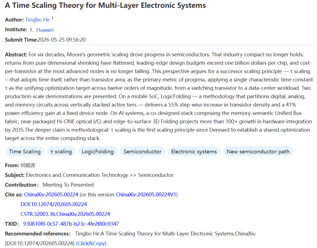
Three Core Upgrades of V2: From Theoretical Framework to Engineering Verification
Compared with the V1 draft released in May, Version 2 features three major upgrades:
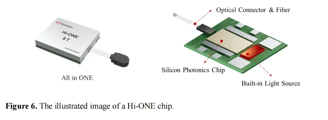
- Complete theoretical system V2 reorganizes scattered discussions into an 8-chapter complete structure with clearer hierarchical logic. It adds schematic diagrams and physical cross-sections of core technologies including the τ multi-layer spatio-temporal model, LogicFolding architecture, bonding interface cross-sections, Unified Bus interconnection architecture, and Hi-ONE optical engine, making the technical roadmap more concrete and traceable.
- First release of mass production test data Critics described V1 as “heavy on theory, light on empirical data”. V2 directly publishes key parameters of Kirin 2026 and the baseline Kirin 9030 Pro under equal performance conditions, including operating voltage, frequency, normalized power consumption, die area, and power density. Real-world performance data from mass-produced chips verifies the engineering applicability of the Tau Scaling Law.
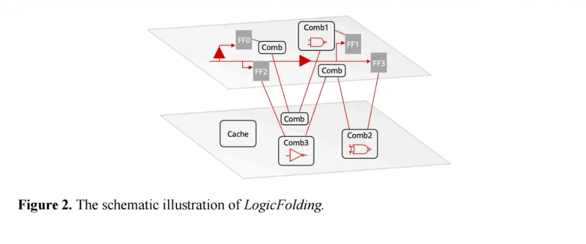
- Refined full-scenario technical evolution roadmap V2 clarifies technical iteration milestones for diverse application scenarios. For mobile terminals, it supplements medium- and long-term evolution paths such as shifting TSVs from top metal layers down to M6 and multi-active-layer stacking, alongside actionable technical scheduling timelines. It also discloses specific performance targets for the next four generations of Kirin processors and Ascend AI chips for the first time.
Released Mass Production Test Data of Kirin 2026
The most widely discussed segment of V2 is the equal-performance benchmark test between Kirin 2026 and its predecessor Kirin 9030 Pro.
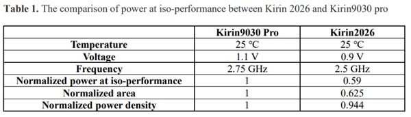
Both chips adopt the same process node: Kirin 9030 Pro uses a traditional planar architecture, while Kirin 2026 leverages LogicFolding. The equal-performance test intentionally lowers Kirin 2026’s operating voltage to match the running performance of Kirin 9030 Pro at reduced power consumption, quantifying efficiency gains brought by LogicFolding.
Test results measured at 25°C ambient temperature are as follows:
- Operating voltage: Reduced from 1.1V (9030 Pro) to 0.9V
- Power consumption: Normalized power drops to 0.59, representing a 41% power reduction
- Die area: Normalized area shrinks to 0.625, a 37.5% area reduction
- Power density: Normalized power density decreases by approximately 5.6%
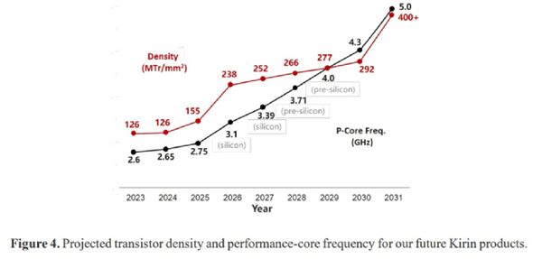
- Transistor density: Rises from 155 MTr/mm² to 238 MTr/mm², a 55% jump — a density leap that previously required three generations of process miniaturization
- Main frequency: At 1.1V supply, CPU performance core frequency climbs from 2.75GHz to 3.1GHz (13% uplift)
- SRAM: Operating frequency improved by over 40%
- Clock network: Clock buffer count cut by more than 50%, clock skew reduced by 25%, wire length shortened by roughly 30%
All performance gaps stem purely from architectural changes, with no new lithography processes deployed. He Tingbo notes in the paper that the current implementation remains conservative: the hybrid bonding pitch stands at 1.5 microns, and folding is only applied to partial critical paths rather than the full chip. This means the published test data does not yet reflect the full potential of LogicFolding.
Full Roadmap Unveiled for Four Generations of Kirin Chips (2026–2029)
V2 publicly releases the long-term iteration roadmap of Kirin chips in semi-official data form for the first time.
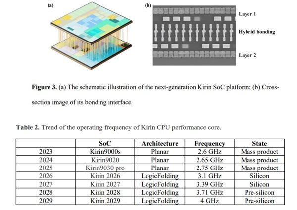
From 2023 to 2025, the Kirin series adopted planar architectures, with CPU performance core frequency rising only from 2.6GHz to 2.75GHz — a cumulative gain of less than 6% across three years. Starting with Kirin 2026’s LogicFolding design, the main frequency jumps directly to 3.1GHz, delivering a single-generation uplift exceeding 12%.
The V1 roadmap ended at 2029 (target 4GHz); V2 extends projections to 2031:
- 2030: Target transistor density of 292 MTr/mm², CPU frequency of 4.3GHz
- 2031: Target density exceeding 400 MTr/mm², CPU frequency of 5GHz
In a May speech, He Tingbo stated that a transistor density of 400 MTr/mm² would deliver equivalent performance to a 1.4nm process node.
Why Huawei Rejected Sequential 3D Integration in Favor of Wafer-to-Wafer Hybrid Bonding
V2 elaborates on the process route selection for LogicFolding. The industry has two mainstream 3D integration approaches:
- Sequential 3D (Monolithic) Integration: Transistors are grown layer-by-layer sequentially on a single wafer, theoretically delivering the highest alignment precision. Huawei ultimately abandoned this path due to poor yield rates: every additional top layer subjects underlying tiers to repeated high-temperature processing, distorting dopant distribution in bottom transistors, lowering carrier mobility, and degrading overall performance.
- Wafer-to-Wafer (W2W) Hybrid Bonding: Two separately fabricated transistor wafers are aligned and directly bonded, with metal pads bonded to metal pads and dielectrics to dielectrics simultaneously across the bonding interface. Through-silicon vias (TSVs) are etched to interconnect circuits on upper and lower layers. Each wafer undergoes independent manufacturing without thermal process compromises between tiers, significantly boosting production yields.
Gear Ratio Defines the Boundaries of 3D Design Space
V2 adds in-depth interpretation of the “Gear Ratio” concept, defined as the ratio between hybrid bonding interconnect pitch and top-level metal line pitch of the chip.
- A high gear ratio creates sparse vertical connections between stacked wafers, limiting design to discrete optimization: engineers manually partition and allocate entire functional modules to individual layers.
- When the gear ratio falls below 3, cross-layer optimization can be performed at the granularity of small circuit units.
- As the gear ratio approaches 1, vertical interconnect density matches the on-chip metal routing density. The two stacked wafers behave like two metal layers on a single die, fully unlocking the architectural advantages of LogicFolding.
Kirin 2026 currently uses a 1.5-micron hybrid bonding pitch. The paper sets a target to drive the gear ratio closer to 1, with future bonding pitches reduced below 1 micron and overlay alignment accuracy (vertical wafer offset) controlled within 0.5 microns.
First Public Address of 3D Folding Packaging Thermal Challenges
V2 directly addresses heat dissipation bottlenecks introduced by stacked 3D folding architectures. Increased stacking layers drastically raise volumetric power density; traditional passive cooling only supports approximately 100 W/cm² power density.
Huawei’s dual mitigation strategy combines:
- Thermal-aware partitioning and floorplanning: Before assigning circuit blocks to vertical layers, thermal power maps are simulated for all modules. High-power sub-circuits are prevented from vertical stacking or adjacent placement to spatially distribute heat sources across three dimensions.
- CVD diamond heat dissipation layers + microscale liquid cooling channels: Chemical vapor deposition diamond layers cover the top and bottom packaging surfaces, with micrometer-scale cooling channels filled with fluorinated liquid running vertically between stacked tiers, then horizontally across the top diamond plate to dissipate heat via expanded contact area. This solution supports up to 300 W/cm² — three times the thermal capacity of conventional passive cooling.
Industry analysts note TSMC is also developing diamond + liquid cooling packaging, with mass production targeted for 2028–2029. Huawei holds a 2–3 year lead in thermal management and folding packaging design.
The AI System Trinity: Unified Bus, Hi-ONE, and 3D Folding
V2 explains how the three core technologies synergize within AI systems, whereas V1 introduced them independently:
- Unified Bus: Replaces repeated protocol conversion between PCIe, NVLink, Ethernet and other standards in traditional AI clusters with a single universal protocol. Each conversion stage adds overhead from data buffering, serialization and handshakes; Unified Bus eliminates these intermediate steps, cutting cross-node communication latency from tens of microseconds to roughly 100 nanoseconds. Huawei internally refers to clusters achieving this latency as a “System-as-One-Chip”.
- Hi-ONE (Near-Package Optical Interconnect Engine): Transmits data via optical signals instead of copper traces. Each module delivers 8 Tb/s bandwidth, extending transmission range from under 1 meter to 100 meters. Instead of power-hungry high-precision DSPs, Hi-ONE adopts lightweight analog equalization drivers and transimpedance amplifiers, trading relaxed bit error rate tolerance for drastically reduced power consumption and cost.
- 3D Folding: Resolves the fundamental “N-squared vs N” structural limitation of packaging. In traditional 2.5D packaging, compute capacity scales with die area (quadratic growth), while memory bandwidth, interconnections and power delivery are constrained to die edges and scale only linearly with side length. 3D Folding relocates these resources from die edges to the full surface, enabling bandwidth and power delivery to scale proportionally with area alongside compute performance.
Ascend Chips to Adopt LogicFolding Circa 2030
For AI computing hardware, V2 outlines the evolution timeline for Ascend accelerators: the Ascend 990 series will integrate LogicFolding for AI workloads around 2030, with hardware integration density projected to grow over 100-fold by 2035.
He Tingbo states in the paper that over 80% of energy consumption in large-scale AI clusters is spent on data movement, and more than 70% of system costs are allocated to data storage. Reducing data transit latency carries equal importance to optimizing raw computation efficiency.
EDA Tools Remain the Top Bottleneck, with a 5–10 Year Technology Gap
Despite extensive engineering progress detailed in V2, He Tingbo identifies Electronic Design Automation (EDA) tools as the primary unresolved challenge. LogicFolding requires design software to treat multi-stacked wafers as a unified entity and execute fine-grained cross-layer allocation at the standard cell level. Domestic EDA tools lag international counterparts by an estimated 5–10 years. Huawei has developed preliminary internal tooling, with full methodological details to be disclosed in future publications.
Industry analysts confirm the Tau Scaling Law has been validated via mass-produced hardware, with its technical feasibility beyond doubt. The core question is whether Huawei’s chip performance under the Tau framework can offset limitations in domestic wafer fabrication, and potentially surpass TSMC and Samsung’s foundry capabilities. Analysts judge He Tingbo’s 2031 target of equivalent 1.4nm density to be conservative, with practical progress likely 1–2 years ahead of schedule.
He Tingbo: Confident of Steady Progress Over the Next 5–10 Years
He Tingbo writes in the paper:
“Over the next five to ten years, we are confident of steady advancement guided by the Tau Scaling Law. Our acceleration trajectory will not fall further behind alternative industry paths — it will only improve.”
She emphasizes that the Tau Scaling Law does not abandon advanced process miniaturization; instead, it delivers sustained performance gains via systematic time optimization while existing process nodes remain fixed.
“The technical framework for the next decade is clearly defined, yet numerous unresolved challenges persist that cannot be overcome by a single enterprise alone. Cross-industry collaboration and co-creation are required across toolchains, industry standards, performance benchmarks, device physics, commercial models and other domains.”
Editor in Charge: Luffy
Sourcse 1: https://www.eet-china.com/news/202607063965.html
Sourcse 2: https://chinarxiv.org/items/chinaxiv-202605.00224
Keywords: #Tau Scaling Law / τ-Law
#LogicFolding
#Wafer-to-Wafer (W2W) Hybrid Bonding
#Sequential / Monolithic 3D Integration
#Gear Ratio (Huawei’s proprietary technical term)
#Unified Bus
#Hi-ONE