Booming demand for AI chips has reignited CoWoS, an advanced packaging technology shelved for over a decade. This article breaks down the core packaging technology powering the global computing revolution.
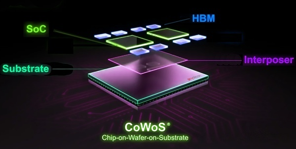
What Is CoWoS?
Short for Chip-on-Wafer-on-Substrate, CoWoS integrates both 2.5D horizontal stacking and 3D vertical stacking architectures, overhauling conventional chip packaging paradigms entirely. By stacking disparate processor and high-bandwidth memory components layer by layer into an interconnected complete system and leveraging Through-Silicon Via (TSV) plus micro-bump (μBump) technologies, CoWoS delivers drastically shortened interconnect routing, lower power consumption losses and markedly enhanced signal integrity versus traditional 2D packaging solutions.
Fundamental Structure of CoWoS
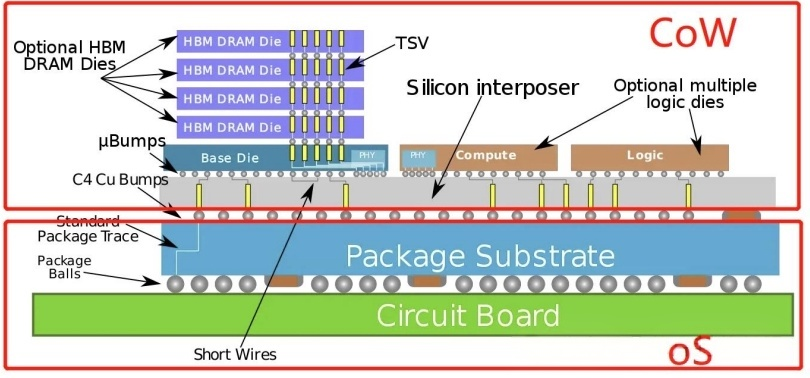
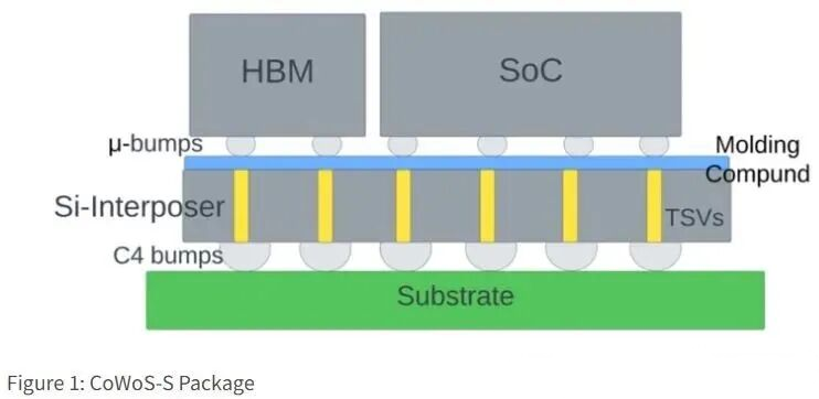
- CoW (Chip-on-Wafer): Multiple dies including logic ICs and High-Bandwidth Memory (HBM) are mounted onto a silicon interposer via μBumps and TSVs to form high-density interconnections.
- WoS (Wafer-on-Substrate): The finished CoW composite module is packaged onto organic substrate, forming a complete packaged component.
Three Major CoWoS Variants Developed by TSMC
TSMC has rolled out three customized CoWoS derivatives tailored to diverse application scenarios:
- CoWoS-S (Silicon Interposer-based): Adopts solid silicon interposer to deliver ultra-high routing density and superior signal integrity, optimized for high-speed high-performance computing workloads3DFabric.
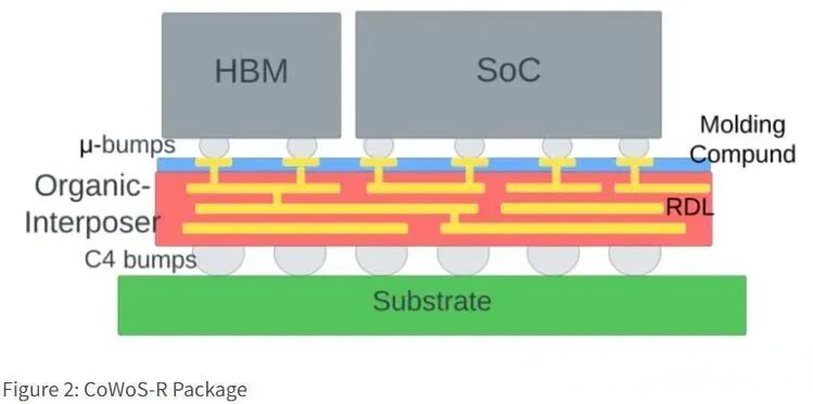
- CoWoS-R (RDL Interposer-based): Replaces costly silicon interposer with Redistribution Layer (RDL) interposer, featuring lower production cost and improved mechanical flexibility at the expense of slightly reduced wiring density.
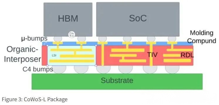
- CoWoS-L: Combines Local Silicon Interconnect (LSI) and RDL technologies for superior flexibility and integration scalability, with capability to integrate up to 12 individual HBM stacks in a single package.
Future Development Roadmap
- Migration toward full 3D packaging: R&D on System-on-Wafer (SoW) technology to integrate full server-grade computing systems onto a single monolithic wafer.
- Technical breakthroughs to overcome existing constraints: Mitigate bottlenecks around oversized interposer fabrication, thermal dissipation and manufacturing yield by deploying hybrid bonding, co-packaged optics, liquid-cooled 3D packaging and other emerging process innovations.
Core Industry Challenges
1. Technical Barriers
Expanding interposer footprint triggers falling fabrication yield and aggravated heat dissipation challenges; taller stacked HBM architectures impose stricter reliability requirements on TSV and micro-bump interconnects.
2. Supply Chain Concentration
Production relies heavily on premium raw materials (silicon wafers, TIM thermal interface materials, specialized RDL films) and dedicated semiconductor equipment; manufacturers across Asia (predominantly Taiwan, China) dominate global CoWoS production capacity.
3. Cost & Mass Production Dilemma
Balancing cost-effectiveness and high-volume mass manufacturing remains a persistent industry hurdle for large-scale commercial adoption.
Key words:
#CoWoS #TSMC #AdvancedPackaging #HBM #AIGPU #HPC #2.5DPackaging #AIChip #SiliconInterposer #RDL #TSV #MicroBump #HeterogeneousIntegration #Chiplet #CoWoS_S #CoWoS_R #CoWoS_L #3DIC #WaferLevelPackaging #HybridBonding #AIServer #LLMChip #CoPackagedOptics #SemiconductorSupplyChain #ChipPackaging
Source: Chip Packaging Frontier Official Account (芯片封装前沿) | By Rocky Fresh