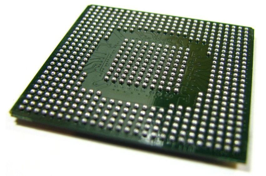
Before we start, let’s take a look at this picture:
Why the Rise of Malaysia and Singapore Matters for Semiconductor Manufacturing
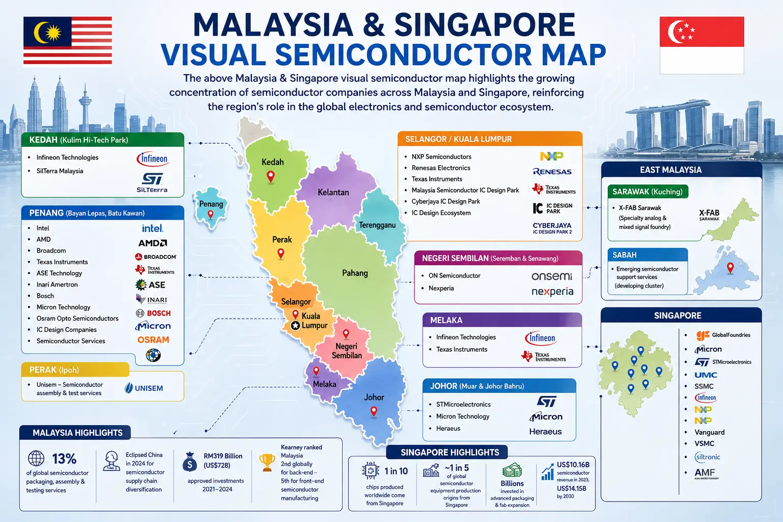
In Southeast Asia, Malaysia and Singapore are rapidly emerging as strategic centers for semiconductor packaging, testing, assembly, wafer fabrication, and advanced chip development.
The above Malaysia & Singapore visual semiconductor map highlights the growing concentration of semiconductor companies across Malaysia and Singapore, reinforcing the region’s role in the global electronics and semiconductor ecosystem.
As demand continues to rise for AI chips, automotive semiconductors, advanced packaging, and high-performance computing devices, both countries are attracting significant investments from global semiconductor leaders.
Malaysia: A Global Hub for Semiconductor Packaging and Testing
Malaysia has long been recognized as one of the world’s most important semiconductor manufacturing locations.
Today, the country contributes significantly to global semiconductor assembly, packaging, and testing operations.
Key semiconductor clusters include:
Penang: Malaysia’s Silicon Valley
Penang remains the country’s most mature semiconductor ecosystem, hosting major operations from:
- Intel
- AMD
- Broadcom
- Bosch
- Micron
- ASE Technology
- Osram
The region has developed a strong supply chain covering:
- IC design
- Advanced packaging
- Test services
- Precision engineering
- Automation solutions
Penang’s ecosystem continues to attract new investments driven by AI, automotive electronics, and industrial semiconductor demand.
Kedah: Expanding Wafer Fabrication Capacity
Kulim Hi-Tech Park in Kedah has become one of Southeast Asia’s most important semiconductor manufacturing zones.
Major players include:
- Infineon Technologies
- SilTerra Malaysia
The region is increasingly focused on:
- Power semiconductors
- Silicon wafer manufacturing
- Automotive electronics
- Energy-efficient chip technologies
The recent expansion of power semiconductor production reflects growing demand from electric vehicle and renewable energy sectors.
Selangor and Kuala Lumpur: Growing IC Design Ecosystem
Malaysia is also strengthening its position in semiconductor design.
The emergence of IC Design Parks and technology clusters around Kuala Lumpur is attracting companies involved in:
- Chip architecture
- Electronic Design Automation (EDA)
- AI semiconductor development
- Advanced packaging technologies
This shift demonstrates Malaysia’s ambition to move further up the semiconductor value chain.
Singapore: Advanced Semiconductor Manufacturing Center
While Malaysia dominates many assembly and testing activities, Singapore focuses heavily on wafer fabrication, advanced manufacturing, and semiconductor R&D.
The country hosts operations from industry leaders such as:
- GlobalFoundries
- Micron
- STMicroelectronics
- UMC
- SSMC
- Vanguard
- Infineon
Singapore has established itself as a critical node for:
- Advanced wafer fabrication
- Memory production
- Specialty semiconductor manufacturing
- Semiconductor research and development
Its highly developed infrastructure, skilled workforce, and strong intellectual property protections continue to attract global investment.
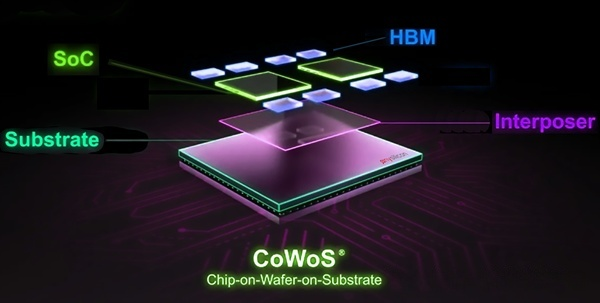
Advanced Packaging Creates New Opportunities
One of the most important trends reshaping the semiconductor industry is advanced packaging.
Technologies such as:
- 2.5D Packaging
- 3D Packaging
- Fan-Out Packaging
- Chiplet Integration
are becoming increasingly important for AI processors, high-performance computing, and automotive applications.
Both Malaysia and Singapore are investing heavily in capabilities that support these advanced packaging technologies.
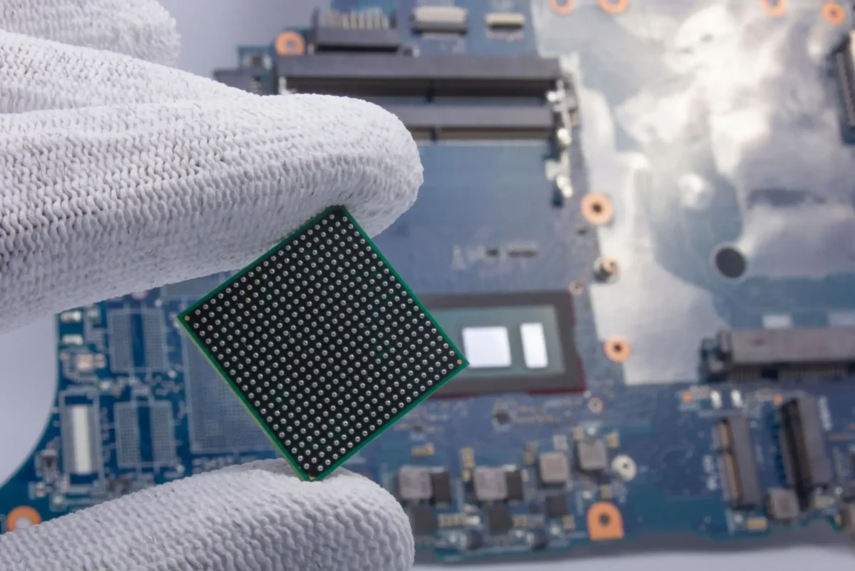
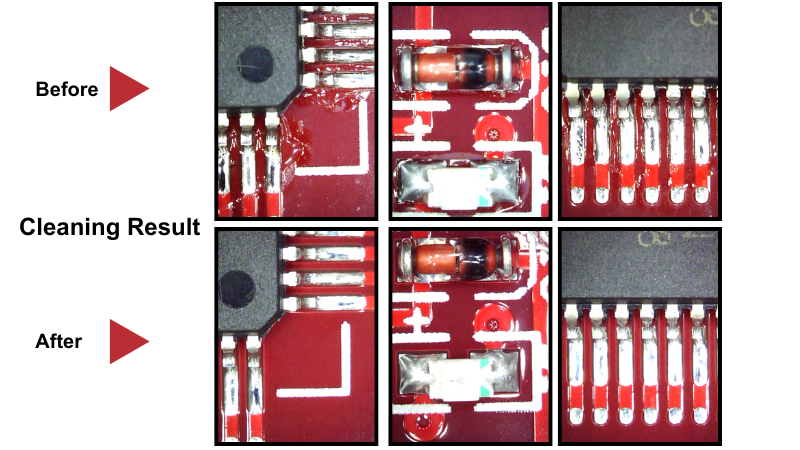
As semiconductor complexity increases, manufacturing cleanliness standards become even more critical.
Why Semiconductor Cleaning Is Becoming a Strategic Process
Advanced semiconductor packaging requires ultra-clean manufacturing environments.
Contaminants such as:
- Flux residues
- Particles
- Ionic contamination
- Organic residues
can negatively impact:
- Wire bonding reliability
- Die attach quality
- Underfill performance
- Long-term device reliability
As semiconductor manufacturers move toward finer pitches and higher integration densities, precision cleaning solutions are becoming an essential part of the production process.
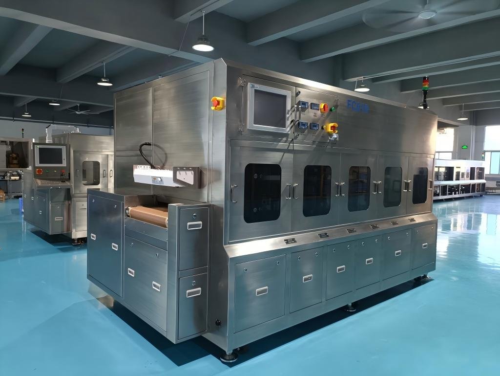
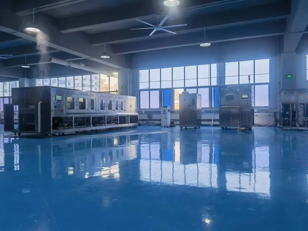
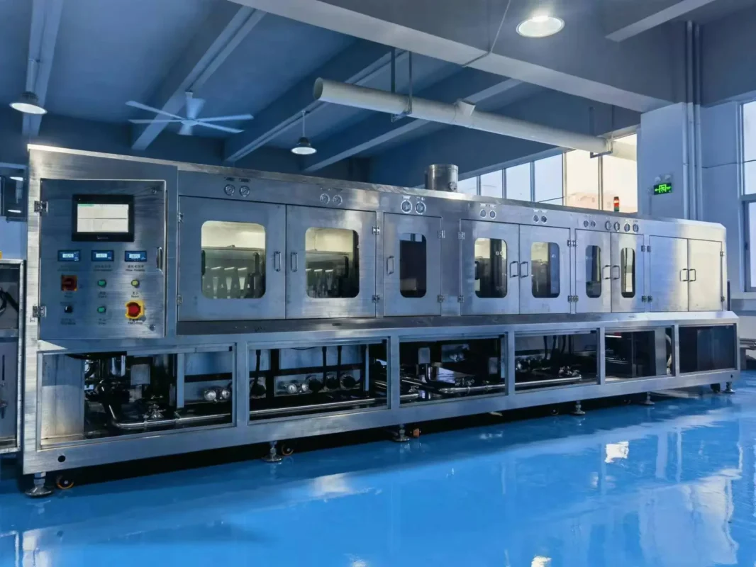
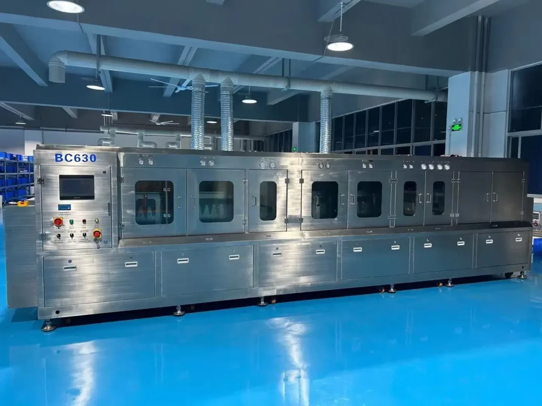
How Spertar Supports Semiconductor Manufacturing
At Spertar, we provide advanced semiconductor cleaning equipment designed for modern packaging and electronics manufacturing facilities.
Our portfolio includes:
- Inline Substrate Cleaning Machine
- Semiconductor Flipchip Package Cleaning Machine
- BGA Ball Mount Flux Cleaning Machine
- Inline Cleaning Equipment for PLP, SIP System in Package, Carrier
- IGBT Inline Ultrasonic Cleaning Machine
These systems help manufacturers improve cleanliness levels, enhance process stability, and support the reliability requirements of next-generation semiconductor devices.
Looking Ahead
The rise of Malaysia and Singapore represents more than regional growth—it reflects a broader shift in the global semiconductor supply chain.
With expanding investments in wafer fabrication, advanced packaging, IC design, and semiconductor manufacturing infrastructure, Southeast Asia is becoming an increasingly important contributor to the future of electronics innovation.
For suppliers, equipment manufacturers, and semiconductor service providers, the opportunities across Malaysia and Singapore are expected to continue growing throughout the coming decade.
Partner with SPERTAR for Semiconductor Cleaning Solutions
Whether you are operating an OSAT facility, advanced packaging line, or semiconductor assembly plant, SPERTAR provides cleaning technologies engineered for the most demanding semiconductor applications.
Explore our semiconductor cleaning solutions and discover how we help manufacturers achieve superior cleanliness, higher yields, and long-term reliability.
Learn more at SPERTAR