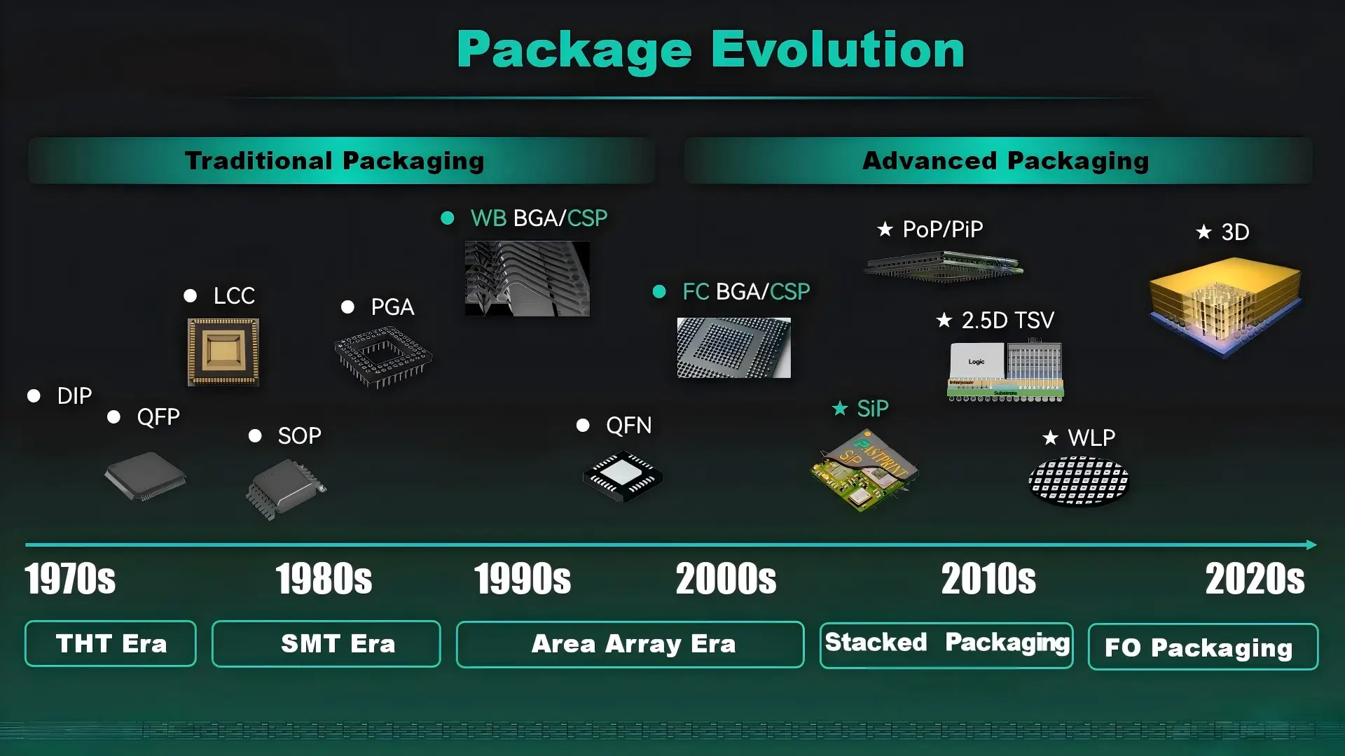
Packaging Evolution and CSP

Chip packaging is a critical segment of the semiconductor industry. It acts as the interconnection channel between the chip and external signals, while providing multiple functions for bare dies, including fixation, sealing, heat dissipation and protection.
In the course of packaging evolution, the industry has undergone the through-hole and surface-mount eras based on leadframe carriers, delivering low-cost and high-reliability packaging solutions. However, leads can only be arranged around the chip periphery, making it impossible to effectively increase the I/O count. To meet the growing demand for improved chip performance, the 1990s entered the era of area array packaging. Initially, leadframe-based QFN was introduced to reduce package footprint. The true area array packaging, nevertheless, refers to substrate-based BGA and CSP. These packages feature area-array surface-mount terminals on the bottom, which greatly improve I/O density, shorten interconnection paths, and expand external I/O channels to hundreds or even thousands.
Over the past two decades, advanced packaging technologies have come into play, starting with FC area array packaging and represented by 2.5D / 3D multi-chip heterogeneous integration. Among them, CSP packaging still plays a vital role.
Concept of CSP Packaging
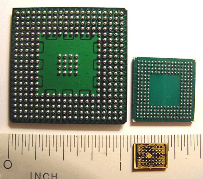
CSP (Chip Scale Package) is defined as chip-scale packaging. Its overall package size is roughly equivalent to the core size of the bare die. Generally, the area ratio of die to package is within 1:1.2. Any package that meets this standard can be classified as CSP.
CSP was first widely adopted in consumer electronic products such as mobile phones. As such products evolve toward multi-function and low power consumption, customers also demand thinner, lighter and more compact devices, requiring high integration of chip packaging. Developed from BGA, CSP perfectly caters to these market demands.
Classification and Typical Applications of CSP Packaging
In terms of physical structure and interconnection methods, CSP is mainly divided into two categories: WBCSP and FCCSP.
For WBCSP, typical types include LGA for fingerprint chips, BOC for DDR chips, and stacked packages for multi-chip memory devices.
In terms of FCCSP, beyond single-die packaging, it also covers MCM for memory, SiP for radio frequency modules, and AiP with integrated antennas.
WBCSP is a highly mature technology. With stable quality and lower cost, it is the preferred option for mass packaging of various chips. From the perspective of technological upgrading, high-end products are increasingly adopting FC solutions. FCCSP delivers significant advantages in expanding I/O scale, enhancing electrical performance, reducing package thickness and improving heat dissipation efficiency.
CSP is widely applied in memories, application processors (AP), radio frequency modules and other fields, covering end products such as smartphones, televisions, video surveillance equipment and automotive electronics.
The FCCSP platform also includes PoP stacked packaging for multi-chip integration, a typical representative of advanced CSP. As shown in the figure below, the upper package adopts four-layer stacked LPDDR memory chips connected to the CSP substrate via wire bonding. The lower package integrates processor or control chips with flip-chip interconnection on the CSP substrate. The two packages are finally stacked and connected by solder pillars.
Summary
As an important form in the development of semiconductor packaging, CSP features thin and compact size, mature manufacturing process, moderate cost and low power consumption, strongly supporting the miniaturization and multi-functional development of electronic products.
Since 2000, CSP has gained increasing popularity in AP, memory, radio frequency, sensors and other fields. Its packaging structure has become more sophisticated, continuously driving the innovation and progress of advanced packaging.
As the core carrier of CSP, CSP substrates are also evolving toward ultra-thin design, fine circuit wiring, multi-layer structure and automated production, to cope with increasingly stringent technical challenges.
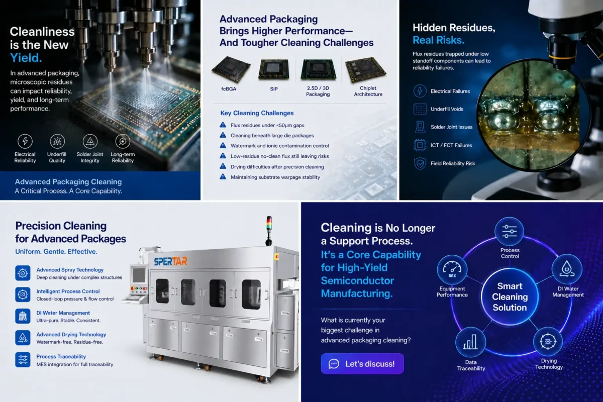
Introduction of Spertar Advanced Packaging Cleaning System
As chip packaging technology evolves rapidly from conventional traditional packaging to high-performance advanced packaging including FCBGA, FCCSP, 2.5D and 3D packaging, high-precision inline cleaning has become an indispensable core process to ensure semiconductor yield and product reliability. To meet the ultra-fine cleaning demands of cutting-edge advanced packaging chips, we proudly present the FC800 FCBGA FCCSP 2.5D/3D Inline Cleaning System, a professional high-efficiency cleaning solution tailored for advanced semiconductor packaging manufacturing.
Core Advantages & System Features of FC800 Advanced Packaging Cleaning System
- Stable PC+PLC integrated control system, equipped with Windows-based English operation interface, ensuring simple operation, stable running and easy production line integration for global factories.
- Adopts an ultra-long chemical washing section with fully adjustable chemical spray pressure and angle, realizing all-round deep cleaning for complex advanced packaging structures.
- Equipped with customized combined spray nozzle kits, specially designed for low-gap FCBGA, FCCSP, 2.5D and 3D chips, solving ultra-fine gap cleaning pain points effectively.
- Reasonable layout of chemical isolation section and powerful air blow section; air pressure and blowing angle are adjustable to remove residual liquid and contaminants efficiently.
- Built-in automatic chemical adding and draining device, realizing unmanned fluid management and improving overall production efficiency.
- Integrated chemical vapor cooling and recovery system, which greatly reduces chemical consumption and cuts down long-term production costs for semiconductor manufacturers.
- Independent chemical temperature cooling system, keeping cleaning solvent at constant optimal temperature to guarantee consistent cleaning quality.
- Real-time inline monitoring system for DI water resistivity and flow rate, strictly controlling cleaning water quality to avoid secondary contamination.
- Extended long rinse section with adjustable DI water spray pressure and angle, ensuring thorough residue rinsing for high-precision chip components.
- Intelligent automatic monitoring system for chemical and water leakage, with real-time fault alarm to ensure equipment safety and workshop production safety.
- Optional chemical concentration real-time detection and auto compensation function, maintaining stable detergent concentration and lowering defective rate.
- Optional SECS/GEM software protocol, supporting intelligent connection with semiconductor MES and factory automation systems to realize smart factory production.
Value for Advanced Packaging Industry
The FC800 inline cleaning machine perfectly matches the manufacturing upgrade needs of modern advanced chip packaging. It covers the whole-process cleaning requirements of FCBGA, FCCSP, 2.5D and 3D packaging chips, balancing high cleaning performance, intelligent control, energy saving and cost reduction. Ideal for semiconductor packaging factories, IC manufacturing plants and high-end electronics production enterprises, it delivers reliable, stable and cost-effective precision cleaning solutions for the next generation of advanced packaging technology.
#Semiconductor Packaging #Leadframe Packaging #Area Array Packaging #WBCSP #FCCSP #PoP Packaging #2.5D/3D Packaging #Chip Scale Package #inline cleaning system #semiconductor cleaning #FCBGA cleaning